-
 The in situ lab is not only fully integrated but service and application support are also included.
 -


Microscopy & Microtechniques
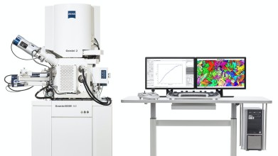
Integrated Solution for Multi-modal In Situ Lab SEM
Mar 29 2022
蔡司将介绍其场发射扫描电子显微镜(FE-SEM)的新集成原位工作流程。当研究人员需要将材料性能与微观结构联系起来时,这对高效开发新材料至关重要,他们现在可以用原位溶液扩展他们的ZEISS FE-SEM进行加热和拉伸实验。这使得他们可以观察金属、合金、聚合物、塑料、复合材料和陶瓷等材料在高温和拉伸下的情况,同时动态地绘制应力-应变曲线。他们可以通过统一的软件环境从一台PC上控制所有系统组件,使无人值守的自动化材料测试长达24小时。学术界、政府和工业界的核心成像设施和材料研究实验室将同样受益于这种新的解决方案。
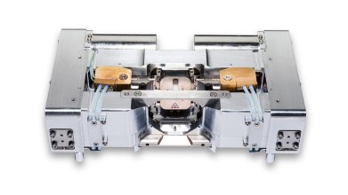
In situ materials testing in the SEM delivers precise measurement of the dynamic response of microstructures to mechanical load under defined temperature conditions. Thanks to the design of ZEISS Gemini electron optics, the integration of in situ hardware is very straightforward. Materials scientists can easily add information such as local chemical composition or crystallographic orientations using combined analytical techniques (e.g., EDS and EBSD). All ZEISS FE-SEMs can be plugged into the ZEISS ZEN core ecosystem, giving users access to ZEN Connect, ZEN Intellesis, and ZEN’s analytical modules, for example.
Dr Michael Albiez, Head of ZEISS Research Microscopy Solutions, commented: “The ability to quantify material microstructure and bulk mechanical properties in a single automated, user-independent experimental environment provides researchers with the tools necessary to design next generation materials for the future low carbon economy. The in situ lab is not only fully integrated but service and application support are also included. What makes our solution unique is that users can define multiple regions of interest (ROIs) and therefore can be sure to never miss interesting areas of their sample.”
The solution is available for immediate upgrade on existing ZEISS GeminiSEM 360 & 460 and ZEISS Sigma 500 microscopes or can be purchased with new systems.
More informationonline


.jpg)
Digital Edition
Lab Asia 29.4 - August 2022
August 2022
In This Edition Chromatography - Automated Sample Preparation:The Missing Hyphen to Hypernation - New Low Volume Air Sampler for PFAS Analysis - Analytical Intelligence Starts with the Samp...
View all digital editions


Events
ACS National Meeting & Expo, Fall 2022
Aug 21 2022Chicago, IL, USA & Online
Aug 22 2022Frankfurt, Germany
Aug 27 2022Maastricht, Netherlands
Aug 28 2022Lisbon, Portugal
Aug 31 2022Singapore